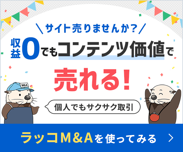


|
Surface Coatings Solve Drift Problems in MEMS
[Home
| Technology | Stiction]
One
of the barriers to full commercialization of complex microsystems is reliability.
Among a number of process related issues, the difficulty in controlling
surface forces is a critical impediment to the fabrication and operation
of MEMS devices. This is a consequence of the scaling law. The surface-area
to volume ratio scales with the inverse of device dimension. As a result,
there are a number of reliability problems related to surfaces; one of
these is Drift.
Drift is a common but hard to deal with problem. As the MEMS industry
matures and more MEMS products come to the market place, how to avoid
or control drift in device performance becomes a pressing issue. One source
of drift is due to charging. which usually leads to instantaneous changes
in driving voltage. Another long term problem is changes in surface characteristics.
We focus on the latter problem here.
One can identity
at least two surface processes that may contribute to drift in device
performance. The first is the effect of adsorption on electrostatic actuation.
Key MEMS materials, such as silicon and silicon nitride, are terminated
by surfaces with high surface energy. This may lead to the accumulation
of background molecules, such as water. The presence of such a thin film
changes the dielectric properties and thus electrostatic actuation. Consider
a parallel-plate capacitive micro-actuator. The normal stress s
for a given driving voltage on the capacitive plate is given by:
where n is
the dielectric constant; V is the applied voltage; d is
the distance between the two plates without bias voltage; and x
is displacement from equilibrium position. The uncontrolled adsorption
of thin molecular films on the surface changes the distance-dependent
profile of dielectric constant and thus, the stress-voltage relationship.
One can estimate the effect as follows: for a gap distance of d = 1 mm
and with the adsorption of a 1 nm thick adsorbate film, the maximum drift
in driving voltage to give the same normal stress is 0.1%. In reality,
the drift is significantly smaller because n is much smaller than the
maximum value, i.e., infinity.
The second and more important effect is adsorption induced change in surface
stress. The surface free energy or interfacial tension, g, is a
function of molecular concentration as given by the Gibbs adsorption equation.
Surface stress (s) is related to g as given by the Shuttleworth
equation:
where e is
the elastic surface strain. Change in s with adorbate concentration is
so significant that it is actually one of the most sensitive mechanisms
for chemical sensing. Both experiment and theory have shown that the change
in surface stress upon the chemisorption of one monolayer of atoms/molecule
can be as high as a few Newtons per meter. For a typical poly-Si cantilever
with thickness of 1-2 micrometer, this magnitude of change in surface
stress can lead to bending on the order of micrometer. In addition to
surface stress, adsorption can also induce substantial albeit slow chemical
changes, such as oxidation in the near surface region of a microstructure.
This leads to longterm changes in stress and spring constants. Therefore,
uncontrolled adsorption onto the high-energy surface of microstructures
can lead to drift in surface stress and spring constants. This is likely
the main reason for drift in device performance.
To solve the drift problem induced by surface adsorption, one needs to
control the surface chemical properties. This can be achieved by the formation
of low-energy, passivation coatings on the surface. With this goal in
mind, we have developed a number of surface coatings with the following
characteristics: covalently bonded monolayer, low surface energy,
thermally and mechanically stable. The design principle of the coating
process is illustrated in scheme 1. A key component in the coating chemical
is a molecule containing two major parts, R & X. The R group
is selected to provide low surface energy, i.e., "wax" or "Teflon"
like, while the X group is chosen to selectively react with the solid
surface of interest for covalent linkage. The attachment of these molecules
to the solid surface is a specially designed process which provides kinetic
control; the reaction self-terminates after a saturated monolayer coverage
is reached. This is very different from self-assembled monolayers (SAMs).
Such a selective and kinetically controlled reaction ensures that the
coating is uniform and conformal with solid surfaces in a MEMS device.
The thickness of the coating is chosen to be 1-2 nm.

Scheme 1. Design of low energy surface coating for MEMS devices.
R represents a molecular group to give low surface energy and X is a
functional group for selective attachment to the solid surface.
Based on these principles, we have developed a number of surface coatings
for MEMS applications. Coating 1: This coating is applied via gas
exposure in a CVD (chemical vapor deposition) type of reaction for pre-released
MEMS devices. It is ideally suited for bulk-micromachined devices or surface
micromachined devices obtained from dry etch-release. This coating process
is compatible with existing equipment, such as cluster tools, on a fab-line.
The coating is typically applied before packaging. For some applications,
the coating process may be combined with the packaging step. Typical water
contact angle of the coated surface is in the range of 94 100o,
indicating the hydrophobic nature of the surface. The coatings are thermal
stability at temperatures as high as 400oC for brief heating in air or
long term heating in inert environment. Coating 2: This
coating is optimized for thermal stability and is applied in the liquid
phase to a variety of MEMS materials. It is designed for MEMS devices
obtained from aqueous HF etching. After liquid release-etch, the sample
is transfer to a coating liquid for the application of the monolayer coating.
The reaction is again kinetically controlled to achieve conformal coating
and monolayer coverage. The MEMS device is dried after the completion
of the coating reaction. Surface energy and thermal stability are both
similar to those of coating 1. Coating 3: This coating is
specifically designed for silicon based MEMS devices obtained from aqueous
HF release etch. It is optimized for exceptionally low surface energy
(water contact angle in the range of 110 125o) and low friction
coefficient (~0.01). It is ideally suited for p-Si based devices from
surface micromachining. After liquid release-etch, the sample is transferred
to a liquid for the application of the monolayer coating. The reaction
is kinetically controlled to achieve conformal coating and monolayer coverage.
The MEMS device is dried after the completion of the coating reaction.
This coating is thermally stable in air at temperature < 200oC. In
inert atmosphere or vacuum, the coating is expected to withstand temperatures
as high as 400oC.
These passivation coatings have been successfully applied to two MEMS
products for optical applications. Drift in driving voltage is significantly
reduced or eliminated after the application of the low energy passivation
coatings.
|